
The semiconductor industry's next major bottleneck may not be lithography equipment, cleanroom space or even investment capital.
It may be electricity.
As AI, HBM and advanced semiconductor demand accelerates, Korea is preparing some of the largest semiconductor manufacturing clusters ever built. In August 2026, plans for the Yongin semiconductor clusters indicated that approximately 14 GW of electrical capacity could be required by 2041.
That scale changes the meaning of energy efficiency.
Saving electricity is no longer simply about reducing utility bills or carbon emissions. For the next generation of semiconductor fabs, every megawatt saved inside the factory could potentially become electrical capacity available for additional manufacturing equipment.
A Semiconductor Fab Never Really Sleeps
A semiconductor fab operates 24 hours a day, 365 days a year.
Thousands of machines must maintain vacuum, temperature, exhaust, gas conditions and process readiness even when wafers are not actively being processed.
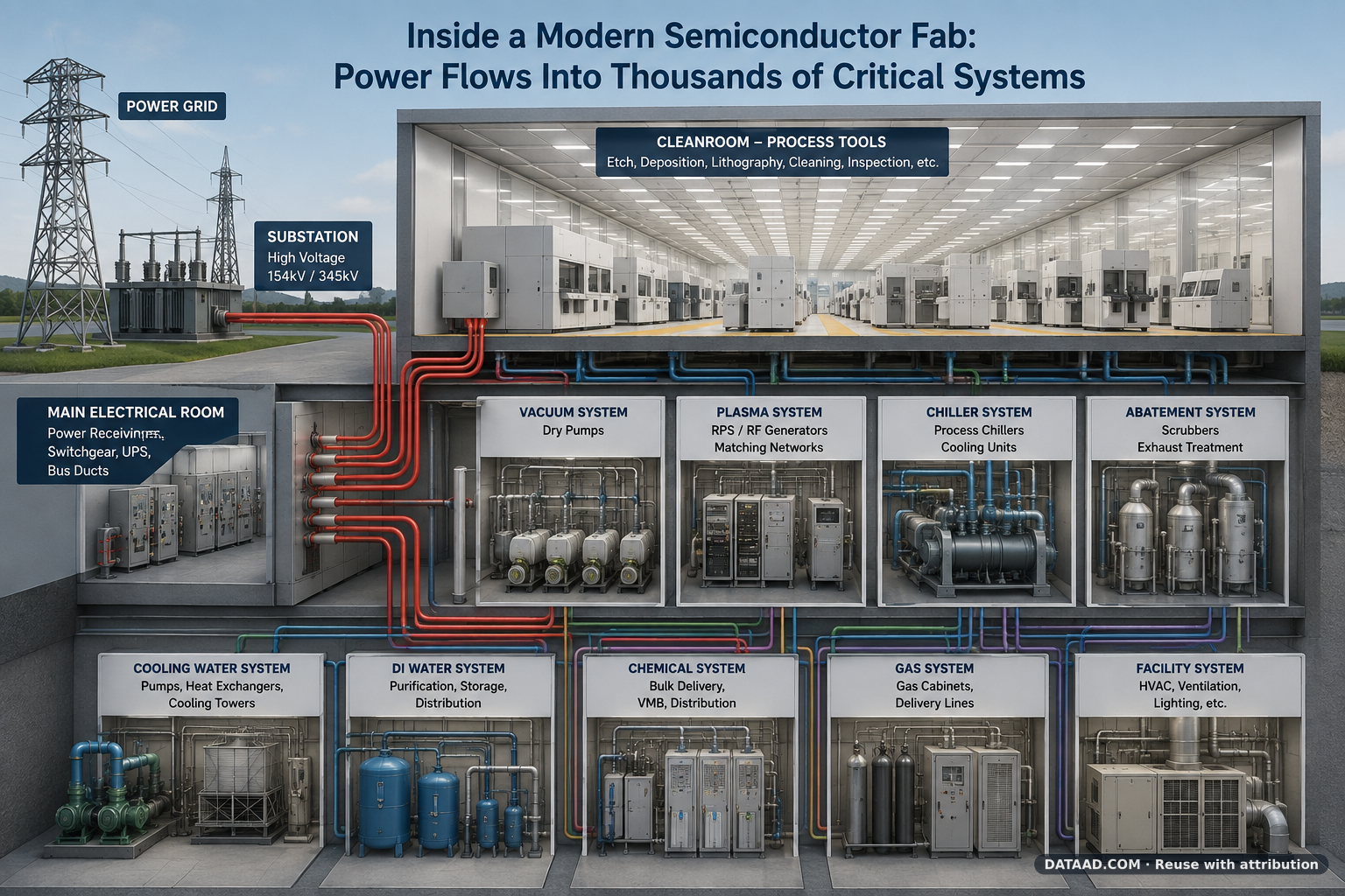
The visible process equipment inside the cleanroom is only one part of this electrical load. Below the cleanroom, the sub-fab contains another enormous collection of equipment:
- Dry vacuum pumps
- Remote Plasma Sources, or RPS
- RF and plasma generators
- Process chillers
- Scrubbers and abatement systems
- Heating systems
- Cooling-water pumps
- Exhaust and ventilation systems
Many of these systems operate continuously.
This means that improving the efficiency of supporting equipment can create savings that multiply across hundreds or thousands of machines.
Electricity Dominates Semiconductor Equipment Energy Use
According to a 2025 SEMI analysis based on 150 field measurement reports, electricity can account for approximately 60% to 90% of the total energy consumption of semiconductor process equipment.
Cooling-water systems can represent another significant energy burden, depending on equipment design and operating conditions.
SEMI also points to a surprisingly simple problem: many semiconductor machines historically had limited low-power operating modes.
A machine might stop processing wafers, but pumps, cooling systems, exhaust equipment and other supporting systems could remain operating near their normal standby condition.
In a factory containing thousands of machines, standby power is no longer a small issue.
Vacuum Pumps: A Major Opportunity for Power Saving
Vacuum pumps are among the most important targets for semiconductor energy reduction.
Etch, deposition, CVD, ALD and many other processes require vacuum, and dry pumps may continue running for long periods to maintain chamber conditions and process readiness.
This creates a simple engineering reality: a small efficiency improvement in one pump may appear insignificant, but the same improvement multiplied across hundreds or thousands of pumps can become substantial at fab scale.
Pump manufacturers are therefore increasingly competing on energy efficiency as well as pumping performance and reliability.
For example, Edwards states that its low-energy iXM semiconductor dry-pump technology can reduce input power by up to 60% in applicable configurations. This is a product-specific manufacturer claim rather than a universal fab-wide saving, but it clearly demonstrates the direction in which the industry is moving.
Plasma Is Essential — But Plasma Requires Power
Advanced semiconductor manufacturing increasingly depends on plasma.
Etching, deposition, chamber cleaning and exhaust-gas treatment can all involve plasma-based technology.
That means power consumption is not limited to the main process chamber.
An advanced process tool may be connected to multiple electrical systems including:
- RF generators
- Matching networks
- Remote Plasma Sources
- Plasma power supplies
- Vacuum pumps
- Plasma-based abatement equipment
Each individual system may represent only part of the tool's electrical demand. Together, however, they create a substantial continuous load.
This is why future plasma equipment development will increasingly require two objectives at the same time:
better process performance and lower electrical consumption.
RPS: Clean the Chamber With Less Energy
Remote Plasma Sources are widely used for chamber cleaning and other plasma-assisted semiconductor processes.
As advanced fabs install more deposition and etch capacity, the number of plasma sources can also increase.
The next stage of RPS development therefore cannot focus only on plasma generation efficiency, cleaning speed and process stability.
Power-conversion efficiency, intelligent standby operation and optimized cleaning cycles will also become increasingly important.
If a plasma source can deliver the same cleaning performance with lower electrical input or shorter operating time, the benefit is multiplied across the entire fab.
RF Generators: Efficiency at the Power-Conversion Level
RF generators transform electrical power into precisely controlled high-frequency energy for semiconductor plasma processes.
As processes become more complex, advanced tools may use multiple RF frequencies and multiple power supplies per chamber.
The opportunity is therefore not simply to reduce maximum RF output. The objective is to improve the efficiency of the complete power-delivery system.
Higher conversion efficiency, faster process control, lower idle consumption and intelligent power management can all contribute to reducing overall fab electricity demand.
Chillers: Cooling Can Consume Electricity Even When the Process Is Idle
Temperature control is another major electrical load.
Process chillers maintain precise temperatures for chambers, RF components and other semiconductor systems. Because temperature stability is directly related to process repeatability, these systems often cannot simply be switched off.
The solution is therefore smarter operation.
Variable-speed compressors, optimized coolant flow, higher-efficiency heat exchangers and intelligent temperature control can reduce unnecessary energy consumption while maintaining process stability.
Samsung Electronics has already disclosed examples of this approach. The company says it has analyzed equipment-level electricity consumption, reduced unnecessary standby operation and changed chiller operating logic so that higher-efficiency chillers receive priority. Samsung has also implemented waste-heat recovery and cooling-tower optimization as part of its energy-saving efforts.
Scrubbers and Abatement: Environmental Protection Also Requires Energy
Semiconductor process gases must be safely treated before they are released.
Abatement systems can use combustion, heating, plasma, water treatment or combinations of these technologies.
These systems are essential for safety and environmental protection, but they can also consume significant amounts of electricity, fuel, water and other utilities.
Future abatement technology must therefore improve destruction efficiency while reducing the energy required per unit of process gas treated.
This creates another important engineering challenge: lower emissions cannot simply be achieved by consuming unlimited energy.
The Most Wasted Electricity May Be Standby Electricity
One of the industry's largest opportunities may not require a completely new machine.
It may require machines to communicate with each other more intelligently.
When a process chamber is not processing a wafer, does the vacuum pump need to run at full operating condition?
Does the chiller require maximum coolant flow?
Does an abatement system need the same operating level?
Does the plasma system need to remain fully energized?
SEMI standards have increasingly addressed these questions through energy-saving and equipment idle modes that allow process tools and supporting sub-fab equipment to coordinate their operating states.
This concept could become increasingly important for future smart fabs.
One Kilowatt Becomes a Megawatt
The mathematics of a large semiconductor fab is powerful.
Consider the engineering model discussed in the previous DATAAD article, with approximately 900 main process tools and hundreds of supporting systems in each major equipment category.
If an efficiency improvement saved just 1 kW per machine across 900 identical supporting machines, the reduction would already be:
900 kW — or 0.9 MW.
If similar improvements are achieved across vacuum pumps, plasma systems, chillers and abatement equipment, the cumulative savings can quickly move from kilowatts to megawatts.
This example is illustrative rather than an estimate of a specific fab, but it demonstrates why equipment-level efficiency matters.
In semiconductor manufacturing, small savings multiplied thousands of times become infrastructure-scale savings.
From Energy Saving to Capacity Creation
This leads to an important change in how the semiconductor industry may evaluate equipment.
| Traditional Equipment Priority | Next-Generation Priority |
|---|---|
| Process Performance | Process Performance + Energy Efficiency |
| Reliability | Reliability + Low Standby Power |
| Throughput | Throughput per kWh |
| Cooling Performance | Cooling Performance per kW |
| Abatement Efficiency | Abatement Efficiency per Unit of Energy |
| Pump Capacity | Vacuum Performance per kW |
For decades, semiconductor equipment suppliers competed primarily on process capability, uptime, yield and cost of ownership.
Those factors will remain essential.
But a new metric is becoming increasingly difficult to ignore:
How much useful manufacturing work can the equipment deliver for every kilowatt of electricity supplied?
Korea's Semiconductor Expansion Makes This Urgent
The issue is particularly important for Korea.
In August 2026, plans for the Yongin semiconductor complexes indicated that approximately 14 GW of electrical capacity could be required by 2041.
Building semiconductor fabs is therefore no longer only about constructing buildings and purchasing process equipment.
Power generation, substations, transmission lines and the timing of grid expansion are becoming part of semiconductor industrial strategy.
Electricity that does not have to be generated, transmitted and transformed is effectively additional capacity available elsewhere.
This makes equipment efficiency strategically important.
The Greenest Megawatt May Be the One the Fab Does Not Need
Renewable energy, nuclear power, LNG generation, energy storage and expanded transmission infrastructure will all play roles in supporting future semiconductor manufacturing.
But supply-side solutions are only half of the equation.
The other half is reducing demand inside the factory.
A lower-power vacuum pump, a more efficient RF generator, an intelligently controlled RPS, a high-efficiency chiller or an optimized abatement system may appear to be an equipment-level improvement.
Multiply those improvements across thousands of machines, and they become part of the national power equation.
In the next semiconductor era,
energy saving is not simply cost saving.
Energy saving is capacity creation.
The semiconductor industry has spent decades asking how to put more transistors onto a wafer.
The next question may be just as important:
How many more wafers can a fab produce with the same amount of electricity?