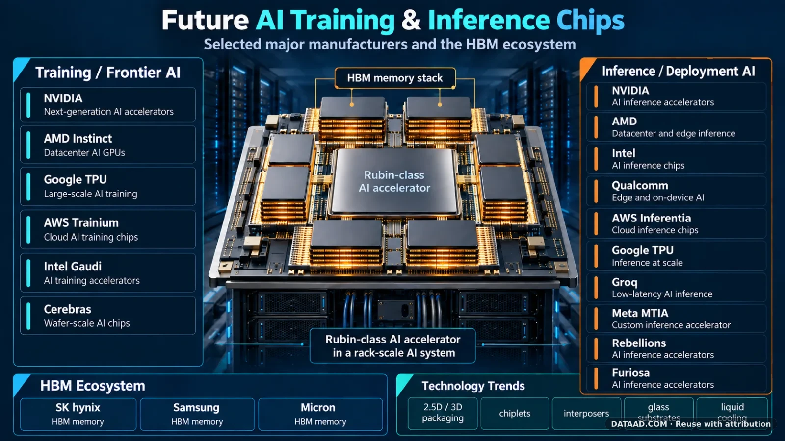
The AI semiconductor race is no longer defined only by smaller transistors.
As AI accelerators combine increasingly powerful GPUs and ASICs with high-bandwidth memory, the semiconductor package itself is becoming a critical part of system performance. Memory bandwidth, interconnect density, thermal control, substrate stability and manufacturing yield now have to be engineered together.
This shift can be seen clearly in three areas: the rapid evolution of HBM, the emergence of glass-based substrates, and the growing importance of specialized advanced-packaging manufacturing equipment.
HBM Is Turning Packaging Into a Core AI Technology
SK hynix provides one of the clearest examples of how memory and packaging are converging.
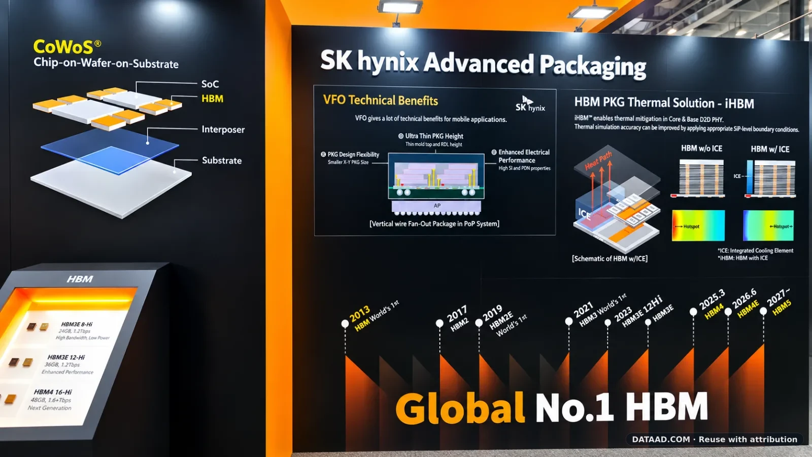
The company traces its HBM technology development back to TSV work that began in 2009. It moved through successive HBM generations, began volume production of HBM3E in 2024, supplied HBM4 samples in 2025 and announced shipments of 12-layer next-generation HBM4E samples in 2026.
The significance goes beyond higher memory capacity. HBM vertically stacks multiple DRAM dies and places them close to high-performance logic. This architecture reduces the distance data must travel and provides the extremely high bandwidth required by modern AI accelerators.
But as more dies are stacked and compute power rises, packaging becomes increasingly difficult. Micro-bump integrity, TSV connectivity, warpage, underfill, thermal resistance and assembly yield can all affect the final performance of an AI processor.
SK hynix has also highlighted tighter integration between memory and logic as a key direction for future AI systems. In 2026, the company introduced its iHBM thermal concept, illustrating another major trend: cooling is beginning to move from the system level directly into the package architecture.
Why Glass Is Entering Advanced Packaging
The next challenge is the substrate underneath the processor and HBM.
Conventional organic package substrates remain widely used, but future AI packages are becoming larger and more complex. More chiplets, more HBM stacks and finer interconnects create increasing demands for dimensional stability, routing density and control of package deformation.
Glass is therefore attracting growing attention as a potential core material for next-generation substrates and interposers.
Glass-based structures can support fine interconnect geometries and through-glass vias, or TGVs, while offering characteristics that are attractive for large advanced packages. The transition, however, is not simply a matter of replacing one material with another. It requires an entirely new manufacturing ecosystem capable of handling glass panels, creating vias, depositing conductive metals, forming redistribution layers, curing polymers and completing highly controlled reflow processes.
The Equipment Behind the Package
This is where companies such as Yield Engineering Systems, or YES.tech, enter the picture.
Headquartered in Fremont, California, YES develops semiconductor capital equipment for wafer- and glass-panel-based advanced packaging. Its portfolio illustrates how many manufacturing steps are required after the semiconductor dies themselves have been fabricated.
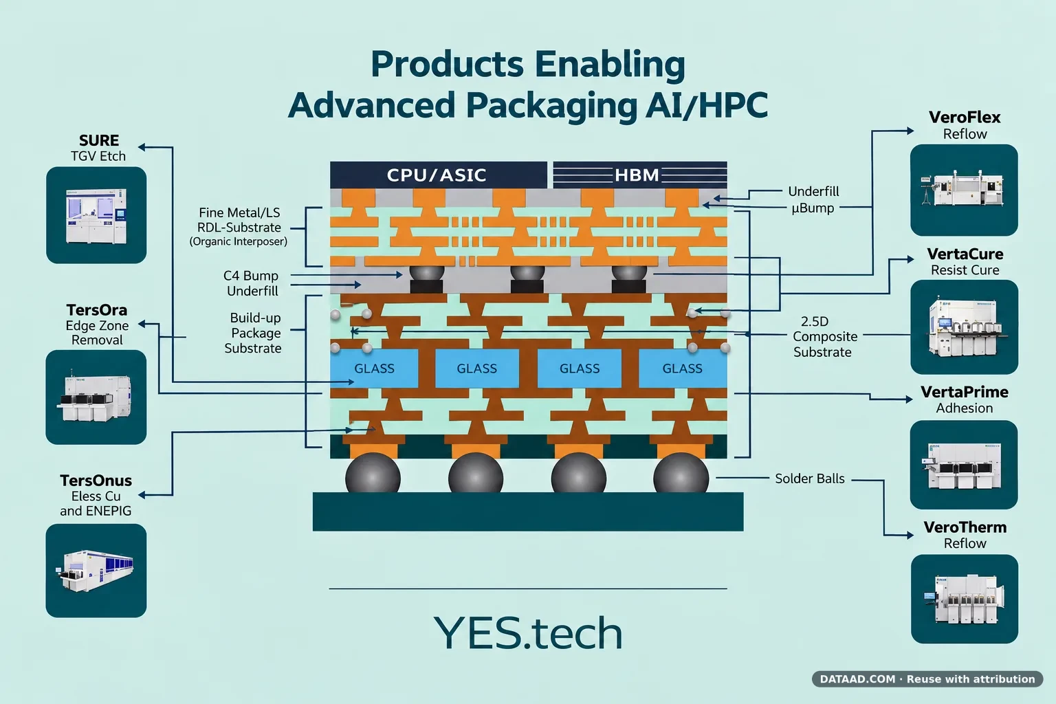
The company positions several equipment platforms around AI and HPC packaging.
- VeroTherm FAR and VeroFlex — reflow platforms used for solder balls, C4 bumps and micro-bumps, including fluxless reflow applications.
- VertaCure — vacuum curing and thermal processing for build-up layers and interposer structures.
- VertaPrime — surface and adhesion treatment designed to improve bonding between build-up layers and substrate cores.
- TersOra — edge-zone removal technology intended to improve uniformity during package build-up processing.
- TersOnus — a wet-processing platform that can support through-glass-via etching as well as electroless copper and ENEPIG-related processes.
Viewed together, these systems show that advanced packaging is not one process. It is a chain of tightly controlled manufacturing steps involving chemistry, heat, vacuum, deposition, cleaning, adhesion and precision material handling.
Glass Packaging Is Moving Toward Production
Glass is also moving beyond the laboratory stage.
In 2025, YES announced orders for dry and wet process systems intended for panel-level manufacturing on glass substrates for next-generation AI and HPC packaging. According to the company, the equipment covers processes including curing, cleaning, reflow and deposition for glass-based 2.5D and 3D integration.
YES separately announced orders for VeroTherm and VeroFlex systems from an unnamed leading global memory supplier. The company said those tools would support 3D stacking of memory and logic chips and sub-10-micron fluxless solder reflow.
These announcements do not establish a disclosed commercial relationship between YES and SK hynix. Rather, they demonstrate the same broader industry direction from two different sides: memory manufacturers are increasing packaging complexity, while equipment suppliers are developing the production tools needed to manufacture those architectures at scale.
From Transistor Scaling to System Scaling
For decades, semiconductor progress was largely described by transistor density and process nodes.
That framework is no longer sufficient for AI.
A modern AI accelerator depends on the interaction of logic dies, HBM stacks, interposers, substrates, micro-bumps, redistribution layers, power delivery and cooling. A weakness in any one of these areas can limit the performance of the entire system.
Advanced packaging is therefore evolving from a back-end assembly step into a strategic system technology.
SK hynix represents the increasing performance demand from the memory side. Glass substrates represent a new materials platform for larger and denser packages. Equipment companies such as YES.tech represent the manufacturing infrastructure required to turn those package concepts into repeatable high-volume production.
The next AI semiconductor breakthrough may therefore come not from one smaller transistor, but from the ability to connect, cool and manufacture an entire package more effectively.
The package is becoming part of the computing architecture itself.