At first glance, semiconductor fabs across Korea, Taiwan and Japan may look remarkably similar.
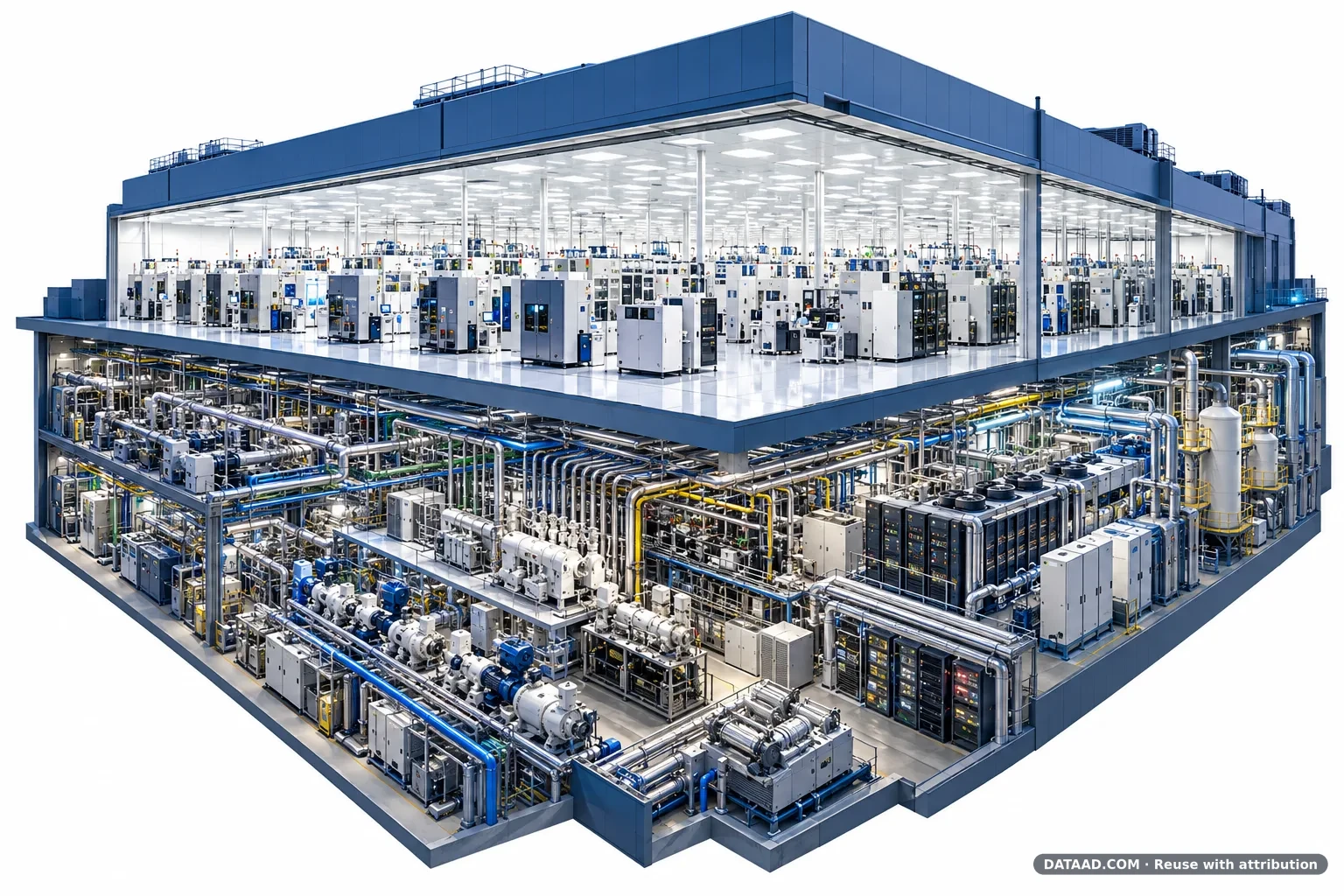
Inside the cleanroom, lithography, deposition, etching, cleaning and inspection equipment operate in tightly controlled environments. Beneath those production floors, however, lies another factory entirely — a dense network of cooling water, ultrapure water, specialty gases, chemicals, vacuum systems, exhaust treatment and electrical infrastructure.
That hidden infrastructure is becoming just as important as the semiconductor tools themselves.
More importantly, fabs are not designed in isolation. Their physical structure reflects what a country produces, how its semiconductor industry is organized, how quickly capacity must be expanded and how suppliers are positioned around the manufacturing site.
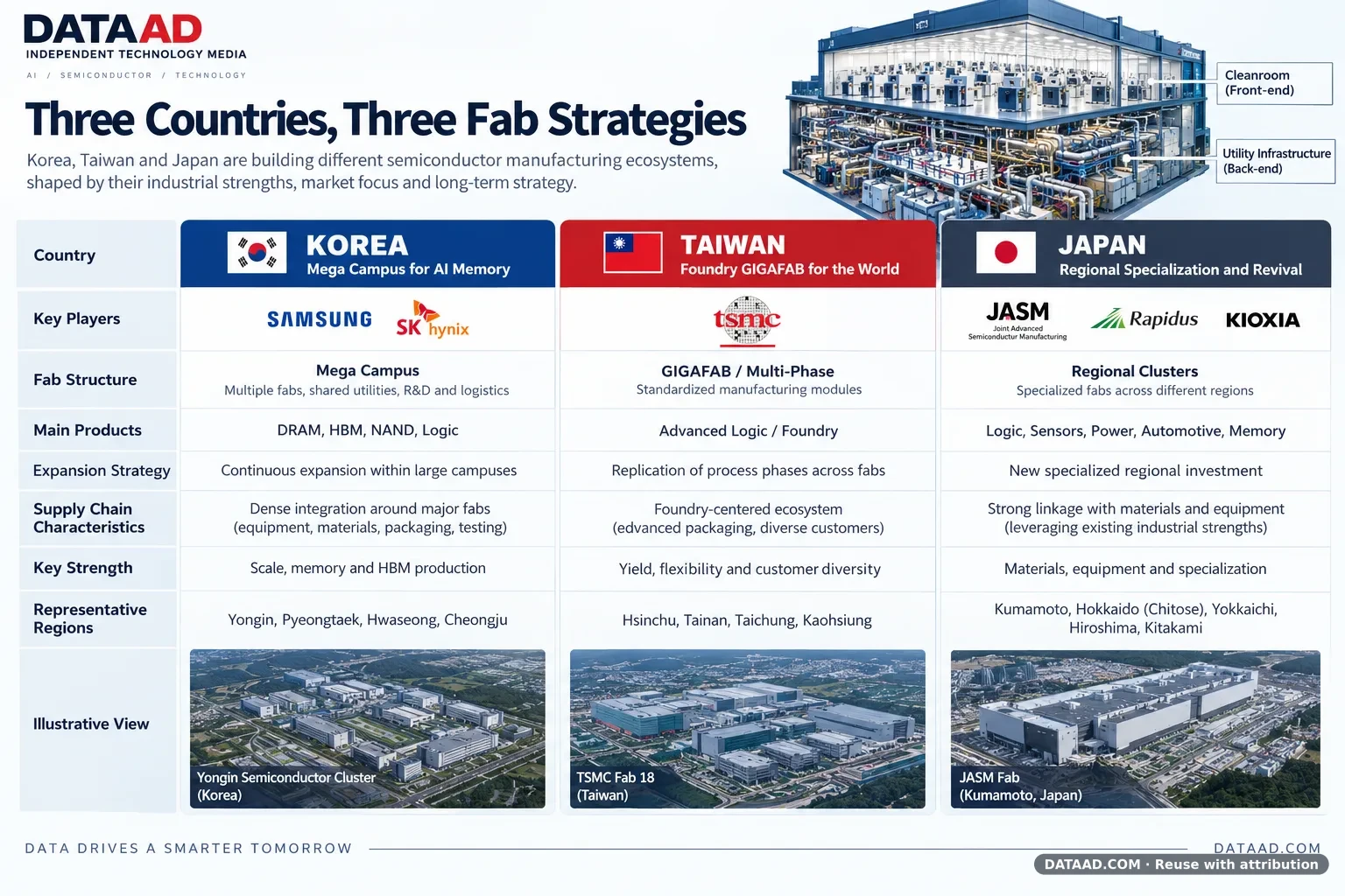
The result is three distinct manufacturing models across Korea, Taiwan and Japan.
Korea: The Mega-Fab Campus
The defining feature of Korea's semiconductor manufacturing structure is scale.
Large production campuses increasingly combine multiple fabs, utility facilities, logistics infrastructure, R&D and future expansion space into a single semiconductor ecosystem.
This structure is closely connected to Korea's global strength in DRAM, NAND and, increasingly, high-bandwidth memory for AI accelerators.
SK hynix, for example, is developing its Yongin Semiconductor Cluster as a sequence of four fabs. In August 2026, the company announced additional investment in Yongin Y2 and Cheongju M17 to expand its long-term production base for AI-era DRAM and NAND demand.
In a large memory-oriented campus, the fab building is only one part of the investment. Centralized electricity, ultrapure water, cooling water, gases, chemicals, waste treatment and other utilities can support multiple production buildings and future capacity expansion.
This makes the Korean model increasingly resemble a semiconductor industrial city rather than a single factory.
Korea's model can be summarized as: Mega Campus + Memory + HBM + Integrated Infrastructure.
Taiwan: The Foundry GIGAFAB Model
Taiwan also operates enormous semiconductor manufacturing sites, but the industrial logic is different.
At the center of Taiwan's ecosystem is TSMC and the pure-play foundry model. Its fabs manufacture products for a broad range of customers across AI accelerators, CPUs, GPUs, smartphones, networking, automotive and other semiconductor markets.
That makes manufacturing repeatability, yield learning and production flexibility particularly important.
TSMC describes Fab 12, Fab 14, Fab 15 and Fab 18 as GIGAFAB facilities. These sites are coordinated through a centralized manufacturing platform designed to improve consistency, production flexibility, yield learning and time-to-volume.
The company is also expanding 2nm manufacturing in Hsinchu and Kaohsiung while continuing to increase advanced packaging capacity across Taiwan.
Rather than viewing each fab as an isolated factory, Taiwan's semiconductor structure is better understood as a network of highly standardized manufacturing phases connected to a dense foundry and packaging ecosystem.
Taiwan's model can be summarized as: Foundry + GIGAFAB + Process Replication + Advanced Packaging.
Japan: A Network of Specialized Semiconductor Regions
Japan presents a different picture.
Its semiconductor industry has traditionally been distributed across multiple regions and specialties, with strong positions in semiconductor materials, manufacturing equipment, image sensors, automotive electronics, power semiconductors and memory.
Now Japan is adding advanced logic manufacturing back into that industrial base.
In Kumamoto, JASM — TSMC's Japanese manufacturing operation — began volume production at its first specialty technology fab at the end of 2024. TSMC has also said that it plans to introduce 3nm technology at JASM's second fab.
In Hokkaido, Rapidus is developing a new advanced logic manufacturing base, supported by substantial Japanese government and private-sector investment.
The result is not simply a copy of Korea's mega-campus model or Taiwan's GIGAFAB structure. Japan is developing a more distributed network in which different regions and companies perform specialized roles within the semiconductor supply chain.
Japan's model can be summarized as: Regional Specialization + Materials & Equipment + Advanced Logic Revival.
Three Countries, Three Manufacturing Models
| Area | Korea | Taiwan | Japan |
|---|---|---|---|
| Primary model | IDM / Memory | Foundry | Distributed specialization |
| Representative players | Samsung, SK hynix | TSMC | JASM, Rapidus, Kioxia and others |
| Fab structure | Mega Campus | GIGAFAB / Multi-Phase | Regional clusters |
| Key products | DRAM, HBM, NAND, Logic | Advanced Logic / Foundry | Logic, Sensors, Power, Automotive, Memory |
| Expansion logic | Large campus expansion | Repeatable manufacturing phases | Specialized regional investment |
| Core advantage | Scale and AI memory | Yield, flexibility and customer diversity | Materials, equipment and specialization |
The Real Fab Extends Below the Cleanroom
The cleanroom is the most visible part of a semiconductor fab, but it represents only one layer of the manufacturing system.
Below and around it are enormous networks for electrical power, process cooling water, ultrapure water, specialty gases, chemicals, vacuum, exhaust and environmental control.
As semiconductor processes become more advanced, these systems become larger, more redundant and more tightly monitored.
A problem in a seemingly ordinary pump, valve, coupling, chiller or cooling-water circuit can affect production equipment worth billions of dollars.
This is why the next phase of semiconductor investment will create opportunities far beyond wafer-processing tools themselves. Utility equipment, thermal management, fluid distribution, contamination control and facility automation are becoming strategic parts of fab competitiveness.
AI Is Changing Fab Infrastructure Again
Artificial intelligence is accelerating this transformation.
In Korea, HBM demand is driving new memory capacity. In Taiwan, AI accelerators are increasing demand for advanced logic manufacturing and advanced packaging. In Japan, AI and economic-security policy are helping drive investment in a new generation of domestic advanced semiconductor production.
At the same time, semiconductor facilities themselves are becoming increasingly dependent on power, water and thermal infrastructure.
The next semiconductor competition will therefore not be determined by nanometers alone.
Power availability, water, cooling capacity, utility reliability, supply-chain density and construction speed will increasingly determine how quickly advanced semiconductor capacity can be deployed.
A Fab Reflects a Country's Industrial Strategy
Semiconductor fabs may use similar production equipment, but they do not follow the same industrial philosophy.
Korea is moving toward mega-campuses built around memory, HBM and large-scale infrastructure integration.
Taiwan continues to refine a foundry-centered GIGAFAB system optimized for advanced logic, repeatable manufacturing and customer flexibility.
Japan is rebuilding a distributed semiconductor network that combines new advanced logic capacity with its longstanding strengths in materials, equipment and specialized semiconductor manufacturing.
The differences can ultimately be seen not only in corporate strategy, but also in the physical architecture surrounding the fab.
To understand the next semiconductor race, we need to look beyond the wafer.
We need to look at the electricity, water, gases, cooling systems, utilities and industrial ecosystems that keep the wafer moving.
That is where the next semiconductor competition among Korea, Taiwan and Japan is already taking shape.
Cover image: Conceptual cutaway of a modern semiconductor fab. The upper level represents wafer-processing cleanroom operations, while the lower section illustrates the extensive cooling, water, gas, vacuum, power and utility infrastructure required to support advanced semiconductor manufacturing.
Sources: SK hynix · TSMC Fab Network · TSMC GIGAFAB · TSMC 2025 Annual Report · Japan METI