
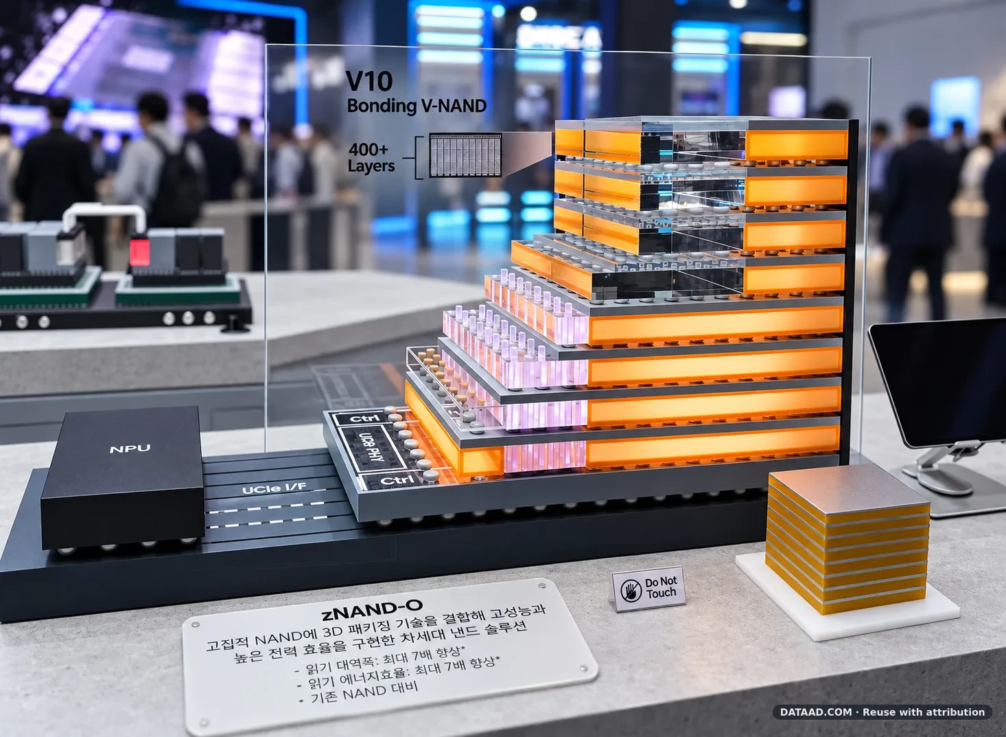
At its booth, Samsung Electronics is showing a physical mock-up of zNAND-O, a next-generation NAND flash concept built for on-device AI. The idea is simple to describe and hard to build: instead of keeping storage far away from the processor, stack the NAND directly on top of a logic die and connect it to the AI processor through a wide, high-speed link.

What the mock-up shows
The display breaks the concept into layers. At the base sits a logic die with a controller (Ctrl) and a UCIe PHY. Above it, multiple NAND dies are stacked vertically, with through-silicon vias (TSVs) running through the stack, shown as transparent pillars in the model. Beside the stack, an NPU connects to it through a UCIe interface, the open standard for linking chiplets.
According to the placard, zNAND-O combines high-density NAND with 3D packaging to deliver:
- Up to 7x higher read bandwidth compared with conventional NAND
- Up to 7x better read energy efficiency compared with conventional NAND
Why it matters: AI models need to live on the device
In today's phones and PCs, NAND storage sits in a separate UFS or SSD package and talks to the processor over a relatively narrow interface. That works for photos and apps, but large AI models need to read billions of parameters quickly and repeatedly. Moving storage physically closer to the NPU, and widening the path between them, is Samsung's answer to that bottleneck.
Samsung plans 4-high and 8-high versions of zNAND-O and is targeting mass production around 2028. The company has also said the approach could deliver the same compute workload at roughly one-sixth the cost of a conventional server setup. That claim has not yet been independently verified.
Built on 400-layer V10 BV-NAND
The foundation of zNAND-O is Samsung's V-NAND technology, and specifically its newest generation: V10 BV-NAND (Bonding V-NAND). It has more than 400 layers and is Samsung's first NAND to use a wafer-bonding architecture. Samsung reports roughly 58% higher storage density than the previous V9 generation, along with improved read, write and I/O performance. Unlike zNAND-O, V10 is close to market.
Part of a larger 3D memory roadmap
zNAND-O was first unveiled at the Future of Memory and Storage (FMS) 2026 conference in Santa Clara in August, alongside zHBM. zHBM applies the same vertical-stacking philosophy to data centers: it places high-bandwidth memory directly on top of an AI accelerator rather than beside it. Samsung claims up to 8x the performance of HBM5, with production expected around 2029.
| Product | Target | Key idea | Timeline |
|---|---|---|---|
| zNAND-O | On-device / edge AI | NAND stacked on logic, UCIe link to NPU | ~2028 |
| zHBM | AI data centers | HBM stacked on top of the accelerator | ~2029 |
| V10 BV-NAND | High-capacity storage | 400+ layers, wafer bonding | Near term |
Competition: HBF from SK hynix and SanDisk
Samsung is not alone in rethinking flash for AI. At the same FMS event, SK hynix and SanDisk announced a standard for High Bandwidth Flash (HBF). The two approaches aim at different places in the system. HBF targets servers, filling the gap between HBM and SSDs. zNAND-O targets end devices, where the goal is faster data exchange between large models and the NPU.
Open questions
- Heat: Stacking NAND on top of active logic exposes it to heat, and NAND data retention degrades at high temperatures. Thermal design will be one of the hardest problems to solve.
- Missing specs: The published figures cover read performance only. Write speed, endurance and capacity have not been disclosed.
- Ecosystem: Because zNAND-O relies on UCIe, adoption depends on whether mobile and PC chip designers build their NPUs to support it.
- Execution: zNAND-O and zHBM are still in development. Whether they reach production on schedule and win customers will be a key test as Samsung competes with SK hynix in AI memory.
The bottom line
zNAND-O is not a product you can buy yet. It is a clear signal of where Samsung thinks on-device AI is heading: devices that keep large models locally and read them almost as fast as memory. If Samsung can solve the thermal and ecosystem challenges, storage could become an active part of the AI compute path rather than a passive warehouse for files.