

Beyond HBM: AI's Next Memory Challenge
The rapid expansion of artificial intelligence is creating a fundamental challenge for semiconductor architecture: computing performance is advancing faster than the memory systems needed to support it.
High Bandwidth Memory (HBM) has become a critical component of modern AI accelerators. By stacking DRAM dies vertically and connecting them through advanced packaging technologies, HBM delivers extraordinary bandwidth within a compact physical footprint.
However, as large language models expand toward longer context windows, multimodal processing, and autonomous AI agents, another limitation is becoming increasingly important: memory capacity.
AI inference must manage not only model parameters but also growing volumes of contextual information, key-value (KV) caches, and frequently accessed data. Increasing HBM capacity alone may not provide the most economical answer.
This is where SK hynix's High Bandwidth Flash (HBF) technology enters the picture.
What Is High Bandwidth Flash?
HBF is an emerging NAND-flash-based memory technology designed to occupy a new performance and capacity tier between HBM and conventional solid-state drives.
Unlike HBM, which uses DRAM, HBF employs vertically stacked NAND flash dies connected through advanced semiconductor packaging and interconnect technologies.
The objective is to combine the density advantages of NAND flash with substantially higher bandwidth than conventional flash storage interfaces can deliver.
SK hynix has presented an HBF architecture targeting significantly greater memory capacity while preserving the high-throughput characteristics required by AI inference applications.
The emerging HBF specifications describe capabilities including:
- High capacity: Up to 512 GB in a specified stacked-memory configuration.
- Vertical integration: Advanced 8-high and 16-high NAND stacking configurations.
- High bandwidth: Performance grades targeting approximately 0.4 to 3.0 TB/s.
- Processor integration: High-speed chiplet interconnect technology for heterogeneous AI computing architectures.
These figures represent emerging specification targets rather than independently verified commercial-product performance.
The significance of HBF is that NAND flash may evolve from conventional storage into a much more closely integrated component of AI computing architectures.
Inside SK hynix's HBF–xPU Architecture
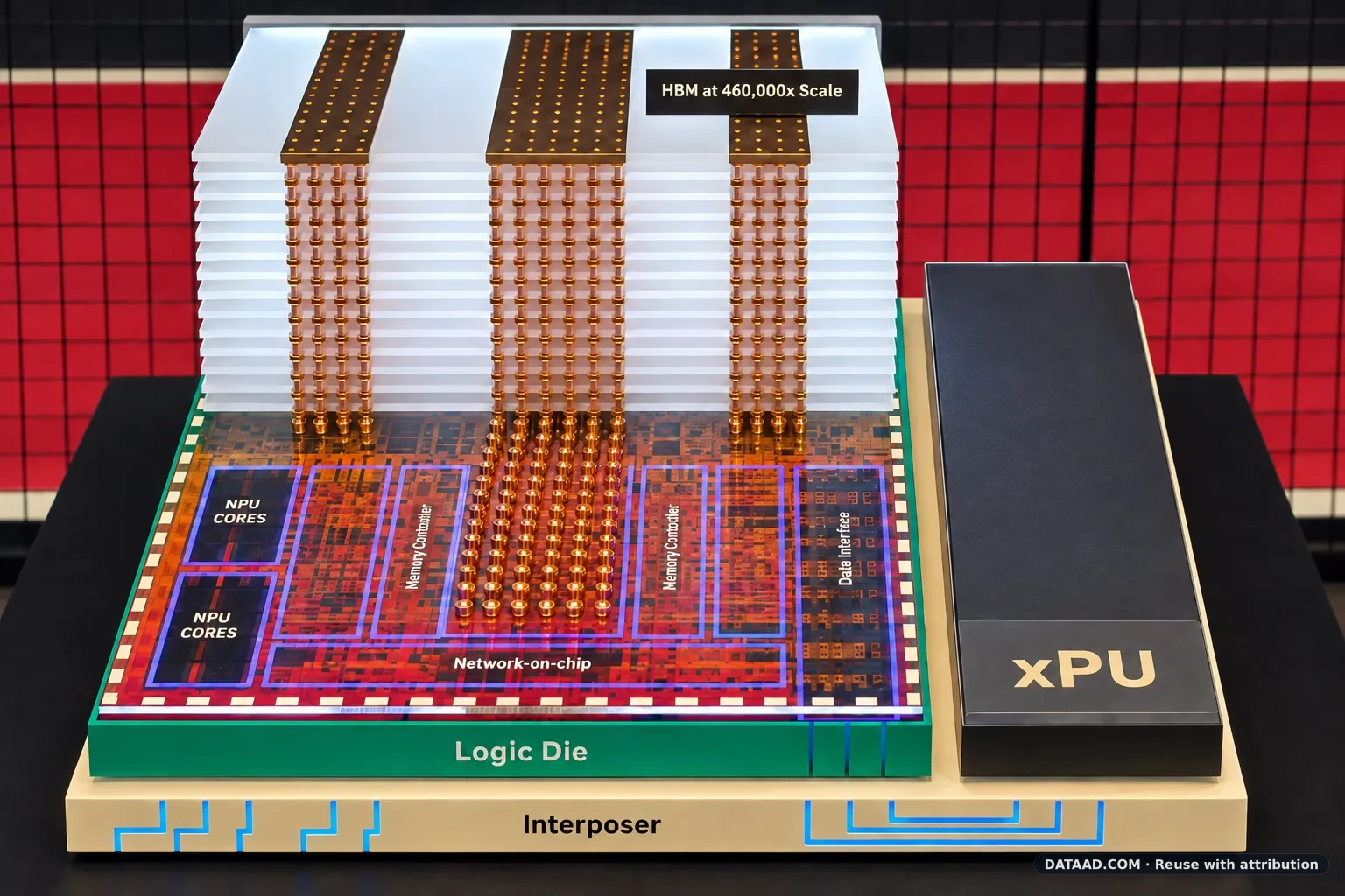
SK hynix's exhibition model illustrates an important direction in advanced semiconductor packaging: bringing large-capacity stacked memory physically closer to AI processing logic.
The conceptual model identifies several architectural components, including:
- NPU cores: Specialized processing elements for artificial intelligence workloads.
- Memory controllers: Circuits responsible for coordinating memory access and data transfers.
- Network-on-chip: An internal communication architecture connecting processing and memory-related components.
- Logic die: The semiconductor layer integrating processing and control functions.
- Interposer: An advanced packaging structure supporting dense electrical interconnections.
- xPU: A generalized processing unit representing heterogeneous AI computing resources.
The model demonstrates how vertical memory integration and advanced packaging can support increasingly complex AI computing systems.
Rather than relying exclusively on separate processor and storage devices, future architectures may bring computing and large-capacity memory into more closely interconnected semiconductor packages.
This could shorten data-transfer pathways, improve effective bandwidth, and reduce some of the overhead associated with moving information between distant components.
However, the exhibition model is an architectural illustration and should not be interpreted as a finalized commercial processor design.
HBM and HBF: Complementary Memory Technologies
HBF should not be viewed simply as a replacement for HBM.
The technologies have different physical characteristics and are more appropriately understood as complementary memory tiers serving different requirements.
| Characteristic | HBM | HBF |
|---|---|---|
| Memory technology | DRAM | NAND flash |
| Primary advantage | High bandwidth and low latency | Higher-density capacity with high read bandwidth |
| Data retention | Volatile | Nonvolatile |
| Principal application | Active AI computation | Capacity-intensive AI inference |
| Key limitation | Cost and capacity scaling | Latency, write endurance and software integration |
| Commercial maturity | Established commercial deployment | Emerging technology |
HBM remains essential where low latency and high memory bandwidth are required for continuously changing computational data.
HBF offers the possibility of accommodating much larger volumes of relatively read-intensive information near AI processing resources.
The important distinction is that high bandwidth does not automatically mean DRAM-equivalent latency. NAND flash retains fundamentally different access, write, and endurance characteristics.
Successful HBF adoption will therefore depend on placing the right data in the right memory tier.
Why AI Inference Changes the Memory Equation
Training large AI models requires tremendous computational capability, but inference creates a different set of technical and economic challenges.
When AI services support thousands of simultaneous users, memory requirements can expand rapidly.
Longer context windows, complex reasoning workloads, multimodal processing, and continuously active AI agents may all increase the volume of information that needs to be retained and retrieved.
Keeping every relevant data structure in expensive HBM is neither practical nor necessarily energy efficient.
A future hierarchical architecture could distribute data across several levels:
- HBM: Frequently accessed computational data and latency-sensitive workloads.
- HBF: Larger-capacity, predominantly read-oriented datasets that benefit from proximity to AI processors.
- System DRAM: Additional working memory and shared computing resources.
- Enterprise SSD: Persistent datasets, model repositories, and bulk storage.
This hierarchy could provide more flexibility in allocating memory resources according to workload characteristics.
For example, certain model parameters and frequently reused datasets could potentially reside in a capacity-oriented memory tier, provided that the processor architecture and software can manage their access efficiently.
Not every workload will benefit equally. Performance gains will depend on access patterns, memory-management software, and the balance between bandwidth and latency.
Advanced Packaging: The Technology Behind Vertical Memory
SK hynix's second exhibition model presents stacked memory as a large three-dimensional structure alongside an xPU module.
Although the display is greatly enlarged for demonstration purposes, it illustrates several important engineering challenges associated with vertically integrated semiconductor devices.
Manufacturing high-density memory stacks requires precise control of semiconductor fabrication and advanced packaging processes.
Key challenges include:
- Wafer and die thinning for compact vertical integration.
- Reliable interconnections between multiple semiconductor layers.
- Thermal management within densely stacked memory structures.
- Signal integrity across high-speed interconnects.
- Manufacturing yield and long-term device reliability.
- Electrical and mechanical integration with AI processors.
As semiconductor architectures become more complex, advanced packaging is emerging as an equally important contributor to system performance alongside process-node improvements.
The future of AI computing will increasingly depend on how effectively memory, logic, and interconnect technologies are integrated into a unified semiconductor platform.
Power Efficiency and AI Data Center Implications
The potential importance of HBF extends beyond semiconductor manufacturing.
Modern AI data centers are facing mounting constraints involving electrical power availability, cooling infrastructure, rack density, and overall operating costs.
As demand for inference expands, increasing the number of AI accelerators and their associated high-performance memory can lead to higher capital expenditure and energy consumption.
If HBF enables certain capacity-intensive applications to operate with less premium HBM, it could potentially improve the economics of serving large AI models.
However, actual energy savings must be demonstrated at the complete system level.
Power consumption depends on numerous variables, including memory access patterns, semiconductor controllers, data movement, packaging, and software efficiency.
The development is also relevant to liquid-cooled AI infrastructure.
More tightly integrated processor-memory packages may increase localized heat density even when they improve overall system efficiency.
Consequently, semiconductor packaging, thermal engineering, and liquid-cooling architecture may become increasingly interconnected design disciplines.
For future AI data centers, improved memory efficiency could influence not only accelerator performance but also the design of server platforms, rack-level power distribution, and cooling systems.
The Road Toward Commercialization
Despite its potential, HBF faces several technical and commercial challenges before it can become a widely deployed AI memory technology.
First, NAND flash latency and endurance characteristics differ substantially from DRAM. A high-bandwidth interface alone cannot eliminate those differences.
Second, software must be capable of allocating data dynamically across different memory tiers without introducing unacceptable performance penalties.
Third, advanced stacking and processor integration must achieve reliable manufacturing yields and commercially competitive costs.
Finally, complete AI computing systems will require extensive validation covering performance, reliability, thermal behavior, and workload compatibility.
Emerging technical specifications and architectural demonstrations represent important progress, but they should not be confused with large-scale commercial deployment.
Real-world benchmarking and production qualification will ultimately determine which AI workloads benefit most from HBF.
DATAAD Perspective: The Next AI Breakthrough May Be About Moving Less Data
The semiconductor industry has traditionally measured technological progress through faster processors, greater transistor density, and higher memory bandwidth.
Artificial intelligence is changing that equation.
As increasingly sophisticated models require larger memory footprints, the physical location of data and the efficiency of moving it are becoming fundamental architectural considerations.
HBM will remain essential for high-performance computing, while HBF introduces the possibility of expanding closely integrated memory capacity using NAND-based technology.
For SK hynix, HBF represents an opportunity to extend its expertise in advanced memory manufacturing into the broader design of AI computing architectures.
The challenge is no longer simply to manufacture faster memory.
It is to determine how different types of memory can operate together to deliver the highest useful computing performance at an acceptable cost and energy budget.
The next major breakthrough in AI infrastructure may come not from computing more, but from moving data more intelligently.
Editorial note: This article analyzes SK hynix's publicly presented HBF technology and exhibition models. Architectural concepts, potential performance benefits, and data-center implications are discussed as technology-development possibilities rather than confirmed commercial-product capabilities.