

Modern semiconductor fabs depend on much more than lithography, deposition and etching equipment. Behind every process chamber is a network of supporting systems that continuously removes chemical residues and keeps the chamber ready for the next wafer.
One of the most important of these technologies is the Remote Plasma Source (RPS), sometimes called a Remote Plasma Generator.
Why Semiconductor Chambers Must Be Cleaned
During processes such as CVD, PECVD and ALD, thin films are deposited on silicon wafers. However, some of the same materials also accumulate on chamber walls, showerheads, electrodes and other internal surfaces.
These residues may include silicon, silicon oxide, silicon nitride and other process materials. If they continue to build up, they can generate particles, reduce process stability and eventually affect semiconductor yield.
For this reason, semiconductor chambers must be cleaned repeatedly during production.
NF₃ and Remote Plasma
Nitrogen trifluoride, or NF₃, is widely used as a cleaning gas in semiconductor manufacturing.
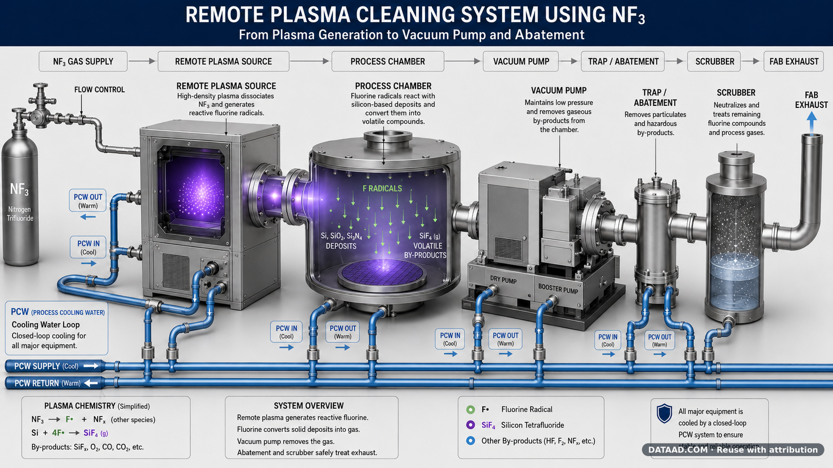
NF₃ is supplied through a controlled gas delivery system into the Remote Plasma Source. Electrical energy then creates a high-density plasma that dissociates the NF₃ molecules and generates highly reactive fluorine species.
A simplified reaction can be expressed as:
NF₃ → Fluorine radicals + nitrogen/fluorine species
Although plasma contains electrons, ions and radicals, remote chamber cleaning relies heavily on reactive neutral fluorine radicals that travel from the plasma source into the process chamber.
Turning Solid Residue into Gas
The fluorine radicals react chemically with silicon-based deposits inside the chamber.
A simplified reaction is:
Si + 4F → SiF₄
Solid silicon residue is converted into volatile silicon tetrafluoride gas. Similar fluorination reactions can remove silicon oxide, silicon nitride and other fluorine-reactive deposits.
This is the key principle of plasma chamber cleaning.
The contamination is not simply collected or absorbed. It is chemically converted from a solid deposit into volatile compounds that can be transported out of the chamber.
The Vacuum Pump Removes the By-products
Once the chamber deposits have been converted into gaseous compounds, the vacuum system becomes critical.
The vacuum pump maintains the low-pressure environment required by the semiconductor process while simultaneously transporting gaseous reaction products away from the chamber.
The overall cleaning process can be simplified as:
NF₃ Gas → Flow Control → Remote Plasma Source → Fluorine Radicals → Process Chamber → Volatile By-products → Vacuum Pump → Abatement / Scrubber
This means that the vacuum pump does much more than simply create vacuum. It is also part of the chemical exhaust transport system of the semiconductor process tool.
From Pump to Scrubber
Exhaust leaving the process chamber may contain silicon fluorides, residual fluorine compounds and unreacted process gases.
These materials must be treated before being released from the fab.
Depending on the equipment configuration, semiconductor exhaust systems may include vacuum pumps, traps and dedicated abatement or scrubber systems.
A typical concept can be represented as:
Process Chamber → Vacuum Pump → Trap / Abatement → Scrubber → Fab Exhaust
The scrubber or abatement system neutralizes or decomposes hazardous chemical compounds before the exhaust is discharged.
Why Use Remote Plasma?
The major advantage of remote plasma technology is that the main plasma-generation zone is located outside the semiconductor process chamber.
Instead of generating highly energetic plasma directly next to sensitive chamber components, reactive fluorine species are created remotely and transported downstream.
This allows chamber cleaning to rely more heavily on chemical reactions while reducing unnecessary direct ion bombardment of internal surfaces.
For increasingly expensive and precise semiconductor equipment, this can contribute to more stable chamber conditions and longer component life.
A Hidden Infrastructure Behind Advanced Chips
A modern semiconductor fab is therefore much more than rows of wafer-processing machines.
Each process tool can depend on multiple supporting systems including:
- Remote Plasma Sources
- Vacuum Pumps
- Gas Delivery and Flow Control Systems
- Traps
- Scrubbers and Abatement Systems
- Chillers
- Chemical Supply Systems
- Fab Utility Infrastructure
All of these systems operate together to maintain the extremely controlled environment required for advanced semiconductor production.
The process can be summarized in four steps:
Remote plasma creates reactive fluorine.
Fluorine converts chamber deposits into gas.
Vacuum pumps remove the gaseous by-products.
Abatement systems treat the exhaust.
As DRAM, NAND Flash, HBM and advanced logic devices require increasingly complex deposition and etching processes, chamber cleaning and exhaust management are becoming even more important.
Remote plasma, vacuum pumps and exhaust treatment systems may remain largely invisible compared with major semiconductor manufacturing equipment, but they are among the critical technologies working continuously behind every advanced wafer.
DATAAD Insight — Semiconductor Infrastructure & Fab Technology