
The center of semiconductor competition is rapidly moving beyond the transistor itself.
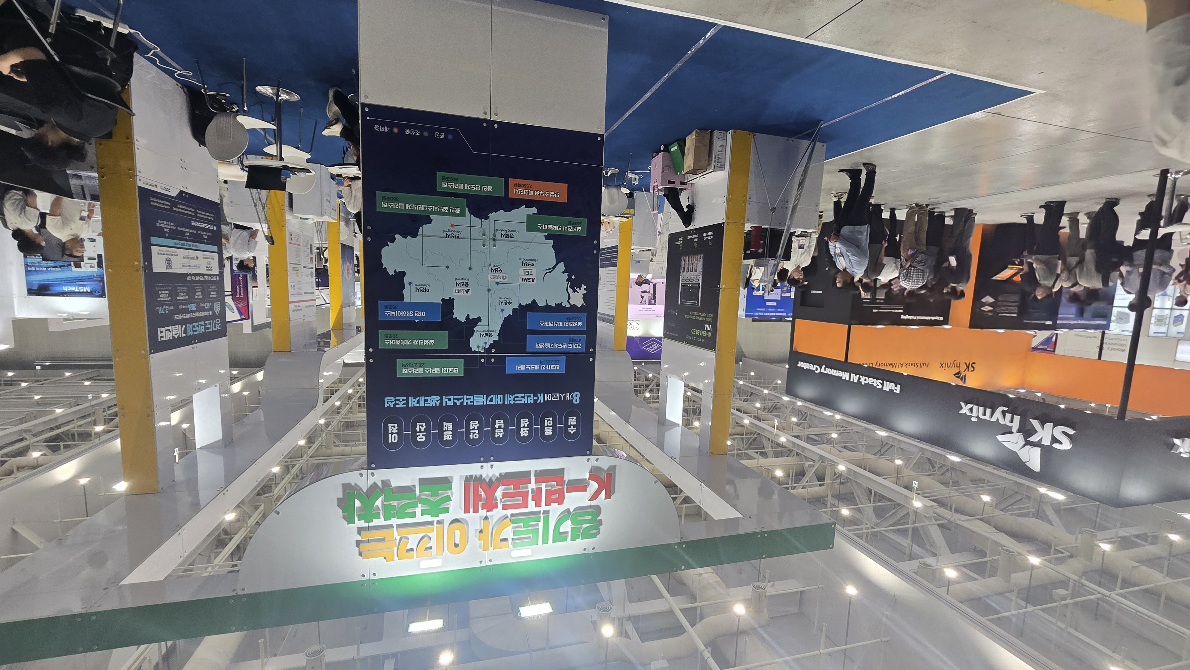
At ASPS 2026 — Advanced Semiconductor Packaging & Chiplet Show, held at the Suwon Convention Center from August 26 to 28, the industry is showing how packaging is becoming a critical part of AI semiconductor performance.
The exhibition brings together semiconductor manufacturers, OSAT companies, equipment makers, materials suppliers and technology developers working across HBM, chiplets, hybrid bonding, advanced substrates, testing and thermal management.
AI Is Changing the Role of Packaging
For conventional semiconductor manufacturing, much of the performance race was driven by smaller process nodes.
AI accelerators are changing that equation.
Modern GPUs and AI processors increasingly combine multiple compute dies, HBM stacks and high-speed interfaces inside one package. The distance between memory and processing units must become shorter, while bandwidth continues to rise.
This makes technologies such as 2.5D/3D packaging, chiplets and hybrid bonding increasingly important.
Packaging is therefore no longer simply the final stage of semiconductor manufacturing. It is becoming part of the architecture of the chip itself.
HBM Makes Packaging a Strategic Technology
The rapid expansion of HBM for AI accelerators illustrates this transition particularly well.
Multiple DRAM dies must be vertically stacked and connected with extremely high interconnect density. At the same time, the HBM stack must communicate with GPUs or other AI processors through increasingly sophisticated interposers and package architectures.
As HBM generations advance, issues including bonding accuracy, signal integrity, power delivery, heat dissipation and package yield become increasingly interconnected.
The boundary between front-end semiconductor processing and back-end packaging is becoming less distinct.
From Chip Cooling to Package Thermal Management
Another increasingly important issue is heat.
Higher compute density and vertically stacked memory mean that thermal management can no longer be considered only at the server or rack level.
Heat must be controlled through several layers:
silicon → package → substrate → cold plate → coolant loop → CDU → facility cooling system.
This is why semiconductor packaging and AI data-center liquid cooling are gradually becoming parts of the same thermal engineering challenge.
A package capable of delivering enormous compute performance is useful only when the heat it generates can also be removed reliably.
Korea's Strategic Position
The location of ASPS in Suwon is significant.

The Seoul–Suwon–Hwaseong–Pyeongtaek–Icheon corridor contains one of the world's densest semiconductor ecosystems, connecting memory manufacturing, foundries, equipment suppliers, materials companies and packaging technology developers.
ASPS 2026 is also being held alongside semiconductor packaging forums, technical seminars, the ISIG Korea executive summit, business matching meetings and semiconductor recruitment programs.
For Korea, leadership in DRAM and HBM creates an opportunity to extend competitiveness further into advanced packaging, substrates, bonding, testing and thermal technologies.
DATAAD Field View
Walking through the technologies represented at ASPS 2026 makes one industry transition particularly clear:
The semiconductor race is shifting from making a single chip smaller to connecting multiple chips more intelligently.
AI performance will increasingly depend on how compute dies, HBM, interconnects, substrates, power and cooling are designed as one system.
In this new semiconductor era, packaging is no longer something that happens after the chip is completed.
The package itself is becoming part of the computer.
DATAAD | Field Report — Suwon, South Korea | August 27, 2026