
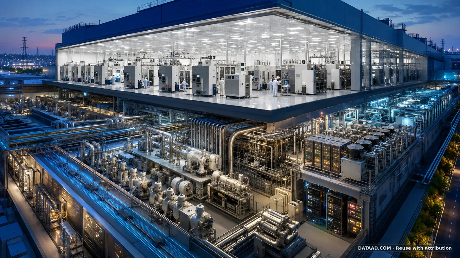
Consider an engineering model of a large semiconductor fab in Pyeongtaek containing approximately 900 major process tools. The actual number of machines supporting those 900 tools can be several times larger than the number of process tools themselves.
The Hidden Factory Behind 900 Process Tools
A modern semiconductor fab can effectively be considered two interconnected factories.
The first is the cleanroom, where wafers move through hundreds of highly controlled manufacturing steps.
The second is the sub-fab, located underneath or adjacent to the process floor, where much of the infrastructure required to operate the production equipment is installed.
| Equipment | Illustrative Installed Base | Main Function |
|---|---|---|
| Main Process Equipment | Approx. 900 | Etch, deposition, cleaning and wafer processing |
| RPS – Remote Plasma Source | Approx. 900 | Plasma generation and chamber cleaning |
| RF / Plasma Generator | Approx. 900 | High-frequency power for plasma processes |
| Vacuum Pump | Approx. 900 | Process vacuum and exhaust handling |
| Process Chiller | Approx. 900 | Precise process and equipment temperature control |
| Scrubber / Abatement System | Approx. 900 | Treatment of hazardous process exhaust gases |
| Total | Approx. 5,400 units | Process equipment plus major supporting systems |
The figures above represent an engineering-scale model and are not an official equipment disclosure by Samsung Electronics. Actual configurations differ according to process technology, equipment supplier, production line and fab design.
RPS: Plasma for Chamber Cleaning
An RPS, or Remote Plasma Source, generates plasma outside the main process chamber and is widely used for chamber cleaning and other plasma-related processes.
During semiconductor manufacturing, process materials gradually accumulate on the internal surfaces of chambers. These residues must be removed regularly because particles and contamination can directly affect process stability and wafer yield.
The RPS is therefore not simply an accessory to the process tool. It is part of the infrastructure required to maintain chamber cleanliness, production repeatability and equipment uptime.
RF Generators: Supplying Power to the Plasma
Many advanced semiconductor manufacturing processes depend on precisely controlled plasma.
An RF generator supplies high-frequency electrical power that creates and controls plasma used in etching, deposition, chamber cleaning and other processes.
As semiconductor structures become smaller and process windows become narrower, stable and precisely controlled plasma power becomes increasingly important.
The process chamber may be where the wafer is physically processed, but the quality and stability of the plasma are heavily influenced by the generator and power-delivery systems connected to it.
Vacuum Pumps: The Heart of the Sub-Fab
Vacuum is essential to many semiconductor manufacturing processes.
Dry vacuum pumps evacuate process chambers, maintain controlled process pressure and continuously remove unused gases and reaction by-products.
These pumps operate for long periods and must handle aggressive gases, particles, powders and condensable materials while maintaining reliable vacuum performance.
For this reason, the vacuum pump is one of the most heavily utilized pieces of equipment inside the semiconductor sub-fab.
Process Chillers: Temperature Is Part of the Process
Semiconductor manufacturing generates significant amounts of heat, while advanced processes often require extremely stable temperature conditions.
This is the role of the process chiller. Unlike conventional building air conditioning, process chillers are directly connected to semiconductor manufacturing equipment and circulate temperature-controlled fluid through chambers, RF systems and other process components.
As semiconductor processes become more sophisticated, cooling is increasingly becoming part of the process itself rather than simply a supporting facility utility.
Scrubbers: Treating Semiconductor Process Exhaust
Semiconductor manufacturing uses reactive, corrosive and greenhouse gases. After passing through the process chamber and vacuum system, these gases cannot simply be released directly into the atmosphere.
Scrubbers and abatement systems decompose, neutralize or remove hazardous process gases before final exhaust.
Depending on the semiconductor process, the system may use wet treatment, combustion, thermal oxidation, plasma or other abatement technologies.
This makes the scrubber an important part of production safety, environmental management and stable fab operation.
900 Process Tools Can Mean More Than 5,000 Machines
This is one of the most important points when trying to understand the real scale of a modern semiconductor fab.
If approximately 900 process tools are installed, an illustrative configuration could include another:
- 900 Remote Plasma Sources
- 900 RF or plasma generators
- 900 vacuum pumps
- 900 process chillers
- 900 scrubbers or abatement systems
That represents approximately 4,500 major supporting equipment units in addition to the 900 primary process tools.
The combined equipment population would therefore reach approximately 5,400 machines.
And this number still excludes many other systems such as gas cabinets, chemical delivery systems, ultrapure-water equipment, cooling-water infrastructure, transformers, power-distribution systems, exhaust systems, sensors, valves, metrology equipment and automated material-handling systems.
A semiconductor fab should therefore not be viewed simply as a building filled with wafer-processing machines.
It is a massively interconnected industrial ecosystem where thousands of machines must operate continuously and simultaneously.
The Next Challenge: Electricity
As semiconductor fabs become larger and more advanced, one of the biggest constraints may no longer be the availability of process equipment alone.
It is increasingly becoming the availability of electric power.
A large fab consumes enormous amounts of electricity, and the process tools are only part of that demand. Thousands of supporting machines in the sub-fab also operate continuously.
Vacuum pumps are particularly important because many of them operate 24 hours a day regardless of whether a wafer is physically being processed at that moment. Even relatively small improvements in pump efficiency can therefore translate into significant electricity savings when hundreds or thousands of pumps are installed in a fab.
The same issue applies to equipment using plasma.
Remote Plasma Sources, RF generators and plasma-based abatement systems all require substantial electrical power. As plasma-based semiconductor processes increase, the electricity consumed by these systems can also become a major part of the overall fab energy equation.
Process chillers add another continuous electrical load because temperature control must be maintained with extremely high precision throughout production.
This means the next generation of semiconductor equipment will increasingly be evaluated not only by process performance, reliability and yield, but also by how much electricity it consumes to perform the same job.
Energy Efficiency May Become a Fab Capacity Issue
This change is important.
Energy efficiency was once discussed mainly as a way to reduce operating costs or carbon emissions. In the era of massive semiconductor fabs and AI-driven demand, it may become something more fundamental: a limitation on how much production capacity can actually be installed and operated.
If electrical infrastructure cannot expand as quickly as semiconductor production capacity, equipment manufacturers will need to reduce the power consumption of individual systems.
Lower-power vacuum pumps, higher-efficiency RF generators, energy-efficient Remote Plasma Sources, optimized chillers and lower-power abatement systems could therefore become increasingly important to future fab design.
For a facility containing thousands of continuously operating machines, saving a few kilowatts at each piece of equipment can eventually become a very large amount of power at the fab level.
The competition surrounding advanced semiconductor manufacturing may therefore move beyond wafer processing technology itself.
The next competition could be about how efficiently thousands of machines underneath the cleanroom can operate.
The cleanroom makes the semiconductor.
The sub-fab makes the cleanroom possible.
And electricity determines how large the next fab can become.
Next on DATAAD
Why Semiconductor Fabs Are Facing a Power Challenge: Vacuum Pumps, Plasma Systems and the Race to Reduce Electricity Consumption
In the next article, DATAAD will examine why electricity availability could become one of the most important constraints on semiconductor fab expansion, and why reducing the power consumption of vacuum pumps, plasma generators, RPS systems, chillers and scrubbers is becoming an important engineering priority for the semiconductor industry.